Nyas
An Android app on Google Play that programs STM32 chips through an ST-Link over USB. No PC, no network.
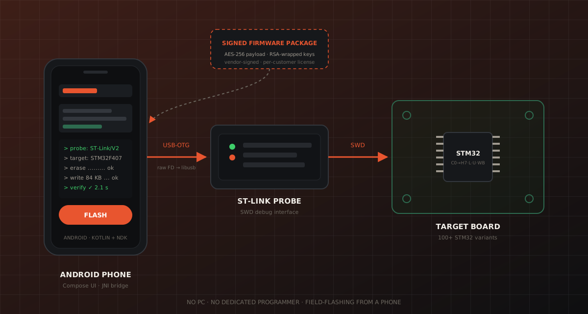
STM32ST-Link (SWD)USB OTGC bridge (stlink, libusb)JNIKotlin app
■ Built under NDA — described at the level the client has published.
The product
Factory and field technicians normally need a laptop, an ST-Link and desktop tooling to flash firmware. Nyas turns an Android phone into that toolchain: plug an ST-Link probe into the phone over USB OTG and write, read, verify and erase STM32 microcontrollers on the spot.
I built the whole stack: the open-source stlink and libusb C libraries compiled from source with the NDK and CMake, the C bridge and JNI layer that Kotlin calls, and the Jetpack Compose app on top. When races showed up on a shared USB session, I rewrote the bridge to be stateless, added erase guards, and reworked the CMake build for LGPL relinking and Google Play's 16 KB pages.
Built for an industrial client. Implementation details are summarised at the level the client has published.
Under the hood
THE ENGINEERING
- 01
Stateless native bridge: every command opens, connects, runs and closes, so a stale USB file descriptor or a shared session can't leak between commands
- 02
Erase guards: a zero address or size is refused instead of falling through to a full-chip wipe, and empty flash and SRAM ranges are rejected
- 03
CMake build reworked so libusb ships as its own shared library (relinkable, as LGPL 2.1 requires) and the native code links with 16 KB page alignment for Google Play
- 04
Caught a release-only R8 issue in development: the C++ looks up the JNI log callback by name, so a keep rule stops R8 from renaming it
- 05
Write .bin and Intel HEX, read, HEX-aware verify, full or sector erase; plugging in a probe auto-detects flash, SRAM, chip ID and the sector map
- 06
Option-byte editor for 6 chip families, including WRP and RDP Level 1 (Level 2 is blocked); batch mode flashes boards one after another and counts pass and fail
- 07
Internal build: encrypted, vendor-signed firmware packages (AES-256 firmware whose key is RSA-wrapped to a device key pair in the Android Keystore), made by a Go command-line tool
- 08
AVR support prototyped in Kotlin (STK500, AVR109 and UPDI engines, 137 tests), not merged into the app yet
- 09
Human-readable log narration: raw probe traffic translated into plain-language steps for technicians
Next case study
Diamond Machine HMI →